Pentek Announces 6.4 GHz A/D and D/A Jade 3U VPX Module for Wideband Defense, Radar and Communication Applications
- Utilizes state-of-art high-speed Texas Instruments A/Ds and D/As
- Matching 6.4 GHz A/D and D/A sampling for wideband signals
- 3U VPX with PCIe Gen.3×8, Optical I/O and RF I/O backplane options
- Jade architecture uses Xilinx Kintex UltraScale FPGA
- Navigator Design Suite supports Xilinx Graphical Vivado IP Integrator
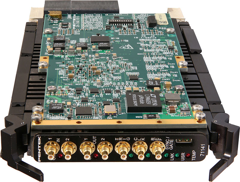
Pentek, Inc., introduced the newest member of the Jade™ family of high-performance data converter 3U VPX modules based on the Xilinx Kintex Ultrascale FPGA. The Model 54141A is a dual channel analog-to-digital and digital-to-analog converter with sample rates up to 6.4 GHz. Programmable DDCs (digital downconverters) and DUCs (digital upconverters) support connections to IF or RF signals.
“The 54141A combines our popular 7114A XMC module with a 3U VPX carrier, yielding a powerful, forward-looking package for very wideband communications or radar applications that require advanced I/O resources,” said Rodger Hosking, vice-president of Pentek, Inc.
Not only does the Model 54141A comply with the VITA 65.0 3U VPX specification, it also offers flexible analog and digital interface options for the VPX P2 backplane connector to meet system-specific requirements. In addition to its PCIe Gen.3×8 interface on the VPX P1 connector, it is possible to add up to 8 more gigabit serial lanes connected directly to the FPGA for supporting user-installed protocols.
The Model 54141A supports the emerging VITA 66.5 optical interconnect standard by providing four optical duplex lanes to a mating spring-loaded backplane connector. With the installation of a serial protocol like 10 or 40 Gigabit Ethernet in the FPGA, the interface enables high-bandwidth digital communications between boards or chassis independent of the PCIe interface.
For flexibility across different I/O requirements, the board can be optioned to support VITA 67.3C. This provides analog signal routing through the VPX backplane to replace front panel connectors for RF In/Out, Sample/Reference clocks and Gate/Trigger/Sync/PPS signals. This option is often required in ruggedized deployments and for simplifying unit field replacements and upgrades.
A/D Stage and Digital Down-converter
The Model 54141A uses the Texas Instruments ADC12DJ3200 12-bit A/D converter with an input bandwidth of 6 GHz, which operates in single-channel interleaved mode with a sampling rate of 6.4 GHz or in dual-channel mode with a sampling rate of 3.2 GHz.
Digital Up-converter and D/A Stage
A Texas Instruments DAC38RF82 D/A with DUC accepts a baseband real or complex data stream from the FPGA and delivers it to the interpolation, up-conversion and dual D/A stages for output signals up to 4 GHz. The two 6.4 GHz 14-bit D/As pair well with the dual input channels while delivering more than twice the output performance of previous generations of Pentek products.
Performance IP Cores
The Model 54141A factory-installed functions include two A/D acquisition modules and a D/A waveform generation IP module. In addition, IP modules for DDR4 SDRAM memories, a controller for all data clocking and synchronization functions, a test signal generator and a PCIe Gen.3×8 interface complete the factory-installed functions. An optional VITA 49.2 data transport protocol IP module conveys digitized signal metadata for signal acquisition and processing elements in communication, radar or storage systems. System integrators get to market with less time and risk, because the Model 54141A can provide a complete turnkey acquisition/generation solution, often without the need to develop FPGA IP.
The Jade Architecture
The Pentek Jade Architecture is based on the Xilinx Kintex UltraScale FPGA, which raises the digital signal processing (DSP) performance by over 50% with equally impressive reductions in cost, power dissipation and weight. As the central feature of the Jade Architecture, the FPGA has access to all data and control paths, enabling factory-installed functions including data
multiplexing, channel selection, data packing, gating, triggering and memory control. A 5 GB bank of DDR4 SDRAM is available to the FPGA for custom applications. The x8 PCIe Gen 3 link can sustain 6.4 GHz data transfers to system memory. Eight additional gigabit serial lanes and LVDS general purpose I/O lines are available for custom solutions.
Navigator Design Suite for Streamlined IP Development
Pentek’s Navigator™ Design Suite consists of two components: Navigator FDK (FPGA Design Kit) for integrating custom IP into Pentek sourced designs and Navigator BSP (Board Support Package) for creating host applications. Users can work efficiently at the API level for software development and with an intuitive graphical interface for IP design. The tools reduce the development time and cost associated with complex designs. The Navigator BSP is available for Windows and Linux operating systems. Unlike others in the industry, Pentek still provides application support to customers at no cost.